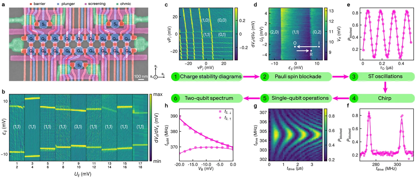
Trending in Mesoscale and Nanoscale Physics
Non-equilibrium bosonization of fractional quantum Hall edges
Edge transport serves as a powerful probe of remarkable low-energy properties of fractional quantum Hall states, including the anyonic character of their excitations. Here, we develop a theory of fractional quantum Hall edges driven out of equilibrium, which is based on the Keldysh action for the bosonized chiral Luttinger liquid. With this non-equilibrium FQH bosonization framework, we first consider a single-mode Laughlin edge and analyze the full counting statistics of charge, the quasiparticle Green's functions, and tunneling transport properties through a quantum point contact, allowing for generic edge excitations. We then extend the formalism to multi-mode edges with inter-mode interactions, and explore, with focus on the $ν=4/3$ and $ν=2/3$ edges as paradigmatic examples, how interaction-induced fractionalization of anyons modifies the edge dynamics and the associated transport observables. While the full counting statistics probes the fractionalized charge of the excitations, the Green's functions and tunneling transport are governed by mutual braiding phases of fractionalized excitations and tunneling quasiparticles. We emphasize in particular the effect of interaction-induced fractionalization on the Fano factor $F$ and the differential Fano factor $F_d$, observables that can be measured experimentally. Our formalism, which provides a unified framework for non-equilibrium transport in FQH edges and Luttinger liquids, permits extracting anyonic braiding information from non-equilibrium edge-transport experiments, and paves the way to various extensions, including more involved experimental geometries and edge structures.
2603.05088
Mar 2026Mesoscale and Nanoscale Physics
Resolution of Topology and Geometry from Momentum-Resolved Spectroscopies
Extracting the complete quantum geometric and topological character of Bloch wavefunctions from experiments remains a challenge in condensed matter physics. Here, we resolve this by introducing the "wavefunction form factor" (WFF) matrix, a quantity directly constructible from intensities in momentum- and energy-resolved spectroscopies like ARPES and INS. We demonstrate that band topology is encoded in "spectral nodes" -- momentum-space points where the WFF determinant vanishes, providing a direct readout of topological invariants via a topological selection rule. Furthermore, when the number of independent probes exceeds the number of the target bands, our framework yields an effective band projector. This enables the determination of Wilson loop spectra and the extraction of an effective quantum geometric tensor, providing a model-independent measurement of the non-Abelian Berry curvature and quantum metric as resolved by the experimental probes.
2601.10677
Jan 2026Mesoscale and Nanoscale Physics
Symmetric approximant formalism for statistical topological matter
The standard approach to characterizing topological matter, computing topological invariants, fails when the symmetry protecting the topological phase is preserved only on average in a disordered system. Because topological invariants rely on enforcing the symmetry exactly, they can overcount phases by incorrectly identifying certain non-robust features as robust. Moreover, in intrinsic statistical topological insulators, enforcing the symmetry exactly is guaranteed to destroy the topological phase. We define a mapping that addresses both issues and provides a unified framework for describing disordered topological matter.
2601.00784
Jan 2026Mesoscale and Nanoscale Physics
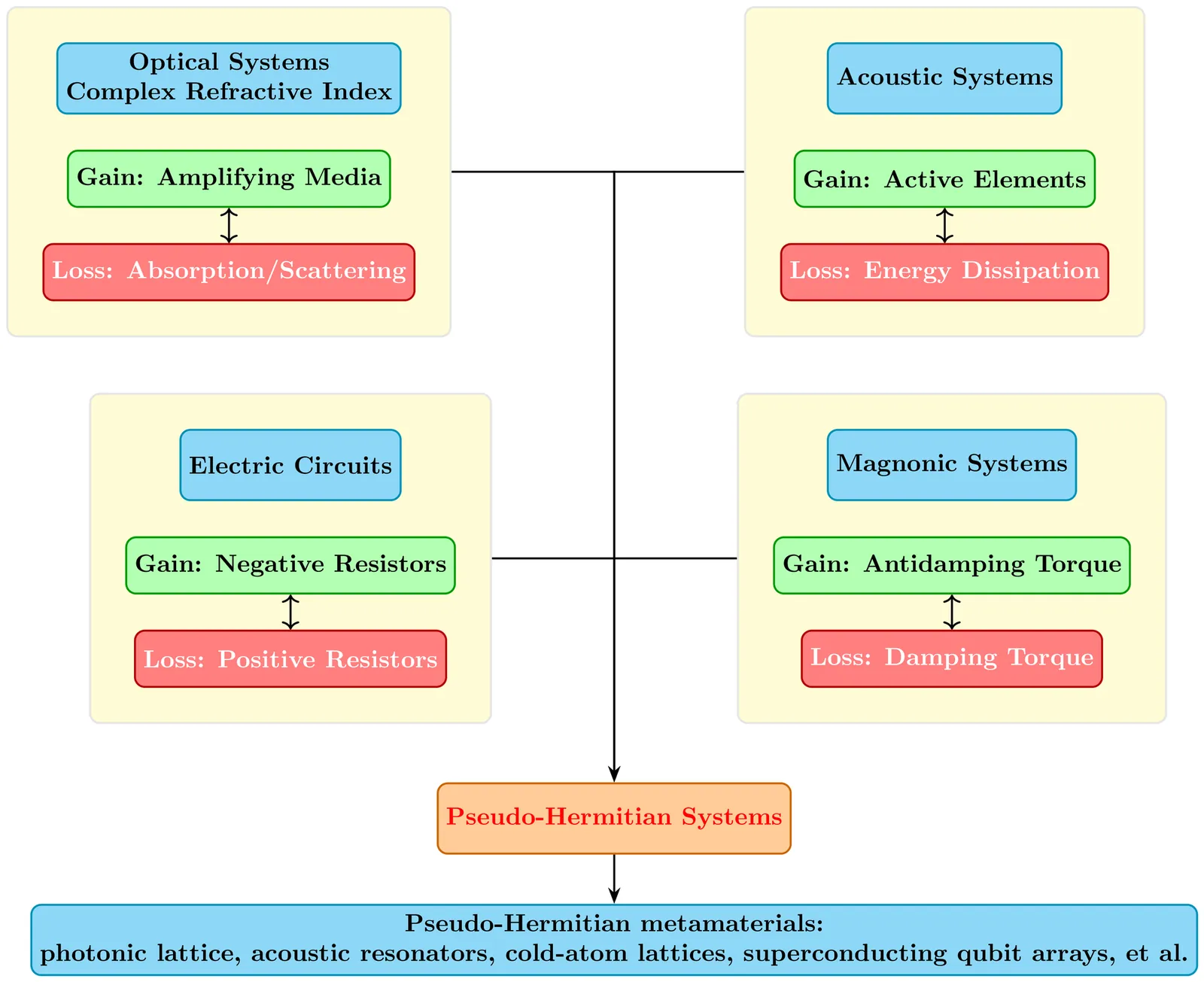
Pseudo-Hermitian Magnon Dynamics
A defining quantity of a physical system is its energy which is represented by the Hamiltonian. In closed quantum mechanical or/and coherent wave-based systems the Hamiltonian is introduced as a Hermitian operator which ensures real energy spectrum and secures the decomposition of any state over a complete basis set spanning the space where the states live. Pseudo-Hermitian, or PT symmetric, systems are a special class of non-Hermitian ones. They describe open systems but may still have real energy spectrum. The eigenmodes are however not orthogonal in general. This qualitative difference to Hermitian physics has a range of consequences for the physical behaviour of the system in the steady state or when it is subjected to external perturbations. This overview reviews the recent progress in the field of pseudo-Hermitian physics as it unfolds when applied to low-energy excitations of magnetically ordered materials. The focus is mainly on long wave length spin excitations (spin waves) with magnons being the energy quanta of these excitations. Various setups including ferromagnetic, antiferromagnetic, magnonic crystals, and hybride structures with different types of coupling to the environments as well as spatio-temporally engineered systems will be discussed with a focus on the particular aspects that are brought about by the pseudo-Hermiticity such as mode amplifications, non-reciprocal propagation, magnon cloaking, non-Hermitian skin effect, PT-symmetric assisted Floquet engineering, topological energy transfer, and field-induced enhanced sensitivity.
2601.00701
Jan 2026Mesoscale and Nanoscale Physics
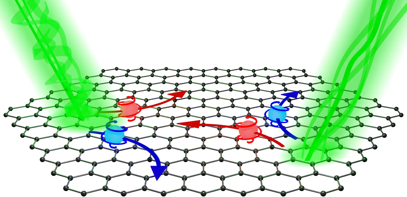
Electric and spin-valley currents induced by structured light in 2D Dirac materials
Structured optical fields can be used for the injection and control of charge and spin-valley currents. Here, we present a systematical study of these phenomena for interband absorption of structured light in 2D Dirac materials. We derive general expressions for the current density and the quasi-classical generation rate of photoelectrons in the momentum, coordinate, and spin-valley spaces. We reveal mechanisms of the current formation determined by the local and non-local contributions to the optical generation, including the mechanisms related to optical alignment of electron momenta by linearly polarized light, optical orientation by circularly polarized light, and the class of charge and spin-valley photon drags sensitive to the phase and polarization profiles of the optical field. We develop a kinetic theory of electric and spin-valley currents driven by the optical field with spatially inhomogeneous intensity, polarization, and phase and obtain analytical expressions for the current contributions. The theory is applied to analyze the photocurrents emerging in TMDC layers and graphene excited by polarization gratings.
2512.11677
Dec 2025Mesoscale and Nanoscale Physics
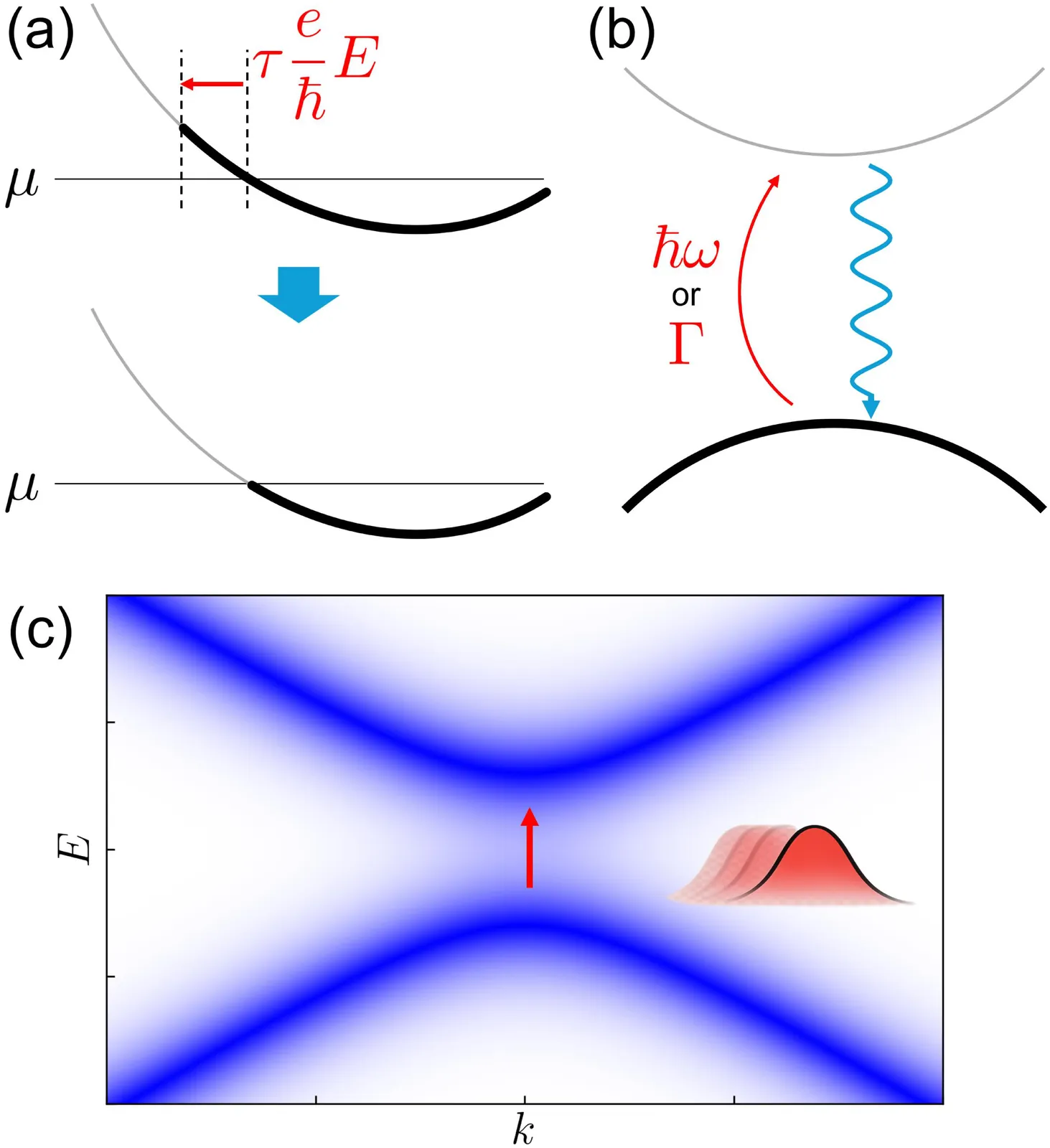
Relaxation to an Ideal Chern Band through Coupling to a Markovian Bath
We propose a microscopic, weak-coupling mechanism by which generic Chern bands relax toward ideal bands. We consider coupling interacting electrons to a Caldeira-Leggett like Ohmic bosonic bath. Using the Born-Markov approximation, Slater determinant states of a Chern band under Hartree-Fock approximation evolve toward Slater determinant states corresponding to an ideal Chern band. We validate our proposal by performing numerical simulation of a massive Dirac model, showing that the Berry curvature and quantum metric indeed co-evolve to saturate the trace condition. Our proposal provides a concrete dissipative route to realize ideal Chern bands, a fundamental building block for the stabilization of fractional Chern insulators.
2511.11394
Nov 2025Mesoscale and Nanoscale Physics
Nearly semi-elliptic relation between the minimal conductivity and Hall conductivity in unpaired Dirac fermions
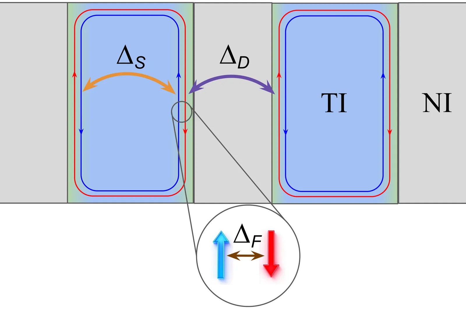
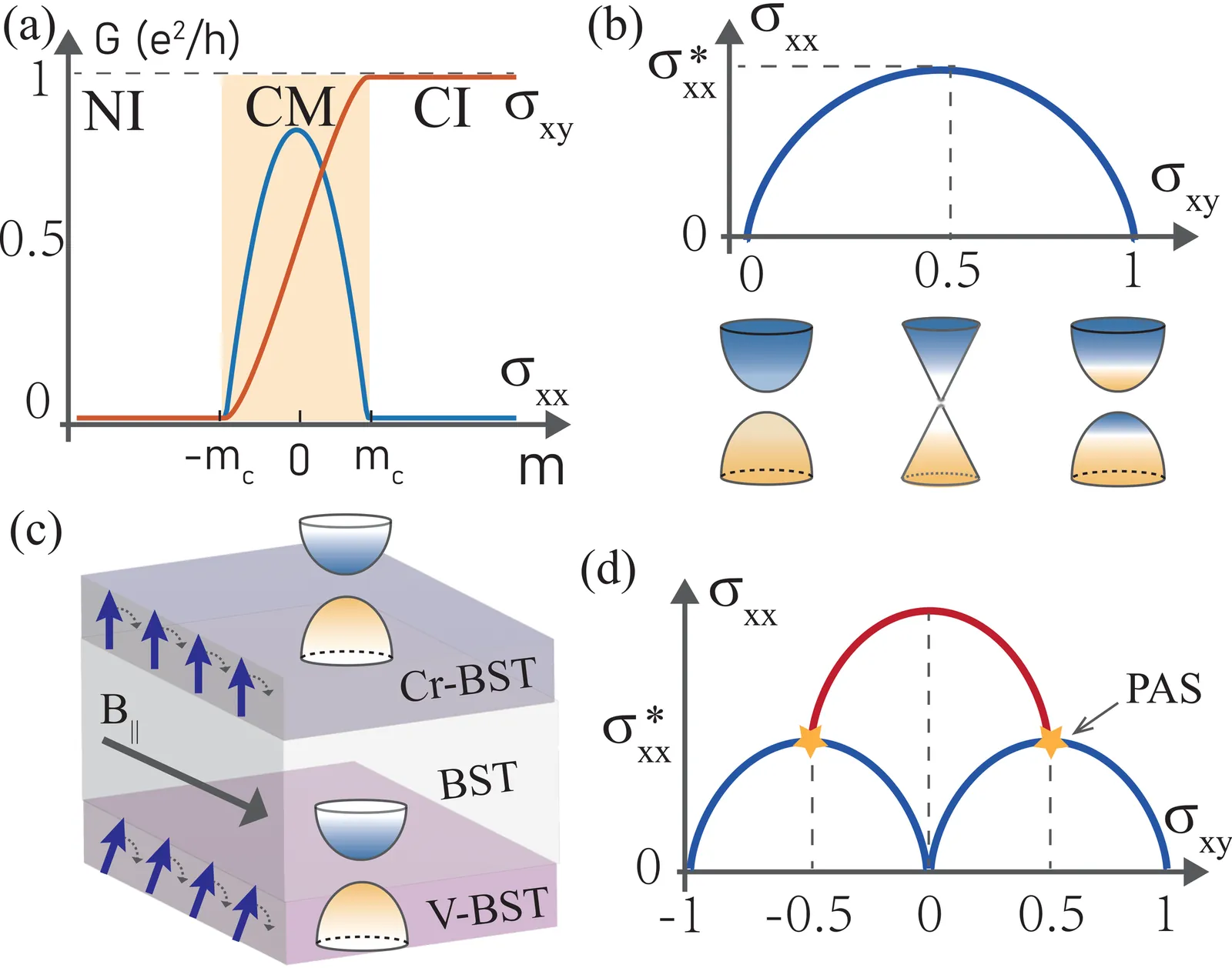
Electric conductivities may reveal the topological and magnetic properties of band structures in solids, especially for two-dimensional unpaired Dirac fermions. In this work, we evaluate the longitudinal and Hall conductivity for unpaired Dirac fermions in the framework of the self-consistent Born approximation and find a nearly semi-elliptic relation between the minimal conductivity and Hall conductivities in the Dirac fermions. Near the charge neutrality point, disorder may drive a metal-insulator transition, and enhance the longitudinal conductivity. For the massless case, the minimal conductivity $σ_{xx}^*$ coexists with the half-quantized Hall conductivity $e^2/2h$, forming an indicator for the parity anomalous semimetal. The relation signals a disorder-induced metallic phase that bridges two topologically distinct insulating phases, and agrees with the recent experimental observation in magnetic topological insulators.
2511.10972
Nov 2025Mesoscale and Nanoscale Physics
Impact of spin-orbit coupling and Zeeman interaction on the subharmonic gap structure due to multiple Andreev reflections in nanoscopic Josephson junctions
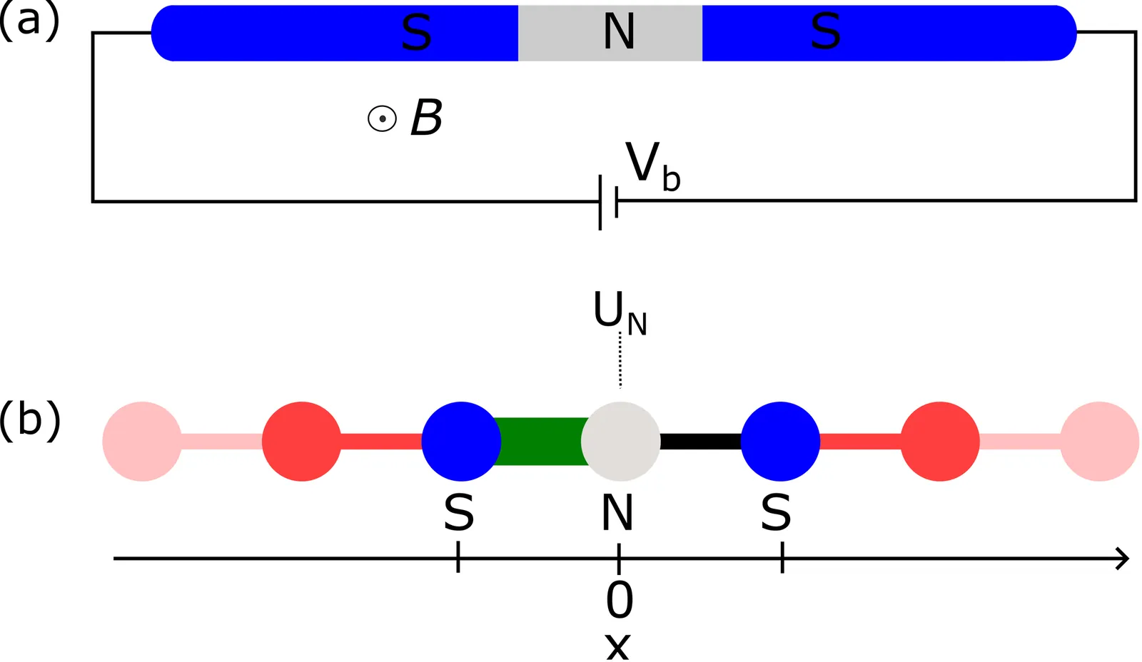
Multiple Andreev reflections in voltage-biased Josephson junctions give rise to the subharmonic gap structure in the conductance, which is widely used to characterize transport properties and estimate the induced gap in the junctions. Here we theoretically investigate the evolution of the subharmonic gap structure in spinful Josephson junctions. Spin mixing introduced by the spin-orbit coupling opens avoided crossings in the dispersion relation of the leads, which, as we demonstrate, subsequently results in pronounced multiple Andreev reflection features in the conductance traces. We analyze how these features evolve under an external magnetic field and explain that their visibility in conductance is governed by the spin polarization of the bands.
2511.11277
Nov 2025Mesoscale and Nanoscale Physics